
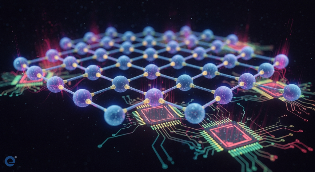
Graphene, a remarkable material, consists of a single layer of carbon atoms. It holds immense promise for revolutionizing the field of electronics. For many years, silicon has been the foundational material for nearly all electronic devices. However, silicon is now approaching its fundamental limits. This creates an urgent need for alternative materials. Recently, researchers at the Georgia Institute of Technology achieved a significant breakthrough. They successfully created the world's first functional semiconductor[1] made from graphene. This development opens entirely new possibilities for creating faster, smaller, and more efficient electronic devices.
The silicon challenge
Silicon has served as the backbone of modern electronics for decades. It powers everything from smartphones to supercomputers. However, the relentless demand for faster computing and smaller devices presents a challenge. Silicon technology is now reaching its physical boundaries. Further miniaturization and performance gains are becoming increasingly difficult. This situation necessitates the exploration of novel materials. These materials must offer superior properties to continue technological advancement.
Graphene's promise and the band gap hurdle
Graphene possesses several extraordinary properties. It is an extremely robust material. It can also handle very large electrical currents. Crucially, it does so without significant heating or degradation. These characteristics make graphene an ideal candidate for advanced electronics. Despite its potential, a major obstacle hindered its use as a semiconductor for decades. This was the absence of a band gap[2]. A band gap is a critical electronic property. It allows semiconductors to switch electrical current on and off. Without a band gap, graphene behaves as a semimetal, not a true semiconductor.
Georgia Tech's groundbreaking achievement
Professor Walter de Heer led a dedicated team at Georgia Tech. They successfully overcame the long-standing band gap problem. Their pivotal research was published in the journal Nature. The team developed a method to produce epitaxial graphene[3]. This involves growing a single layer of graphene on silicon carbide wafers. This specialized growth process chemically bonds the graphene to the silicon carbide. Consequently, the graphene begins to exhibit semiconducting properties. This breakthrough represents a decade of persistent effort. It also involved crucial collaboration with colleagues at Tianjin University in China. This innovation truly throws open the door to a new way of doing electronics.
Superior performance and precise measurement
Proving the functionality of their graphene platform was essential. The team needed to measure its electronic properties without causing damage. They employed a technique called doping[4]. Doping involves adding specific atoms to the graphene. These atoms "donate" electrons to the system. This method confirmed the material's excellent conductivity. Importantly, the doping process did not compromise the graphene's inherent properties. The measurements revealed remarkable performance. Their graphene semiconductor boasts 10 times greater mobility[5] than silicon. This means electrons move through the material with significantly lower resistance. In practical terms, this translates directly to faster computing speeds. De Heer vividly described this improvement. He compared it to "driving on a freeway versus driving on a gravel road" highlighting the efficiency gain.
Industrialization and future prospects
Scientific breakthroughs are merely the first step. Industrialization is crucial for widespread adoption. Black Semiconductor, a spin-off from the Graphene Flagship, is spearheading this effort. They recently secured substantial funding. This includes EUR 254.4 million from various investors. The German federal government and the State of North-Rhine-Westphalia committed significant funds. Additionally, Porsche Ventures and Project A Ventures provided equity funding. Black Semiconductor's primary goal is the mass production of graphene-based chips. This initiative aims to strengthen Europe's technological sovereignty. It will also create numerous high-tech jobs in Germany. Their focus is on developing new chip networks. These networks will solve connectivity barriers. They will also multiply computing power and efficiency.
Implications for material science
This advancement carries profound implications for material science. It promises to enable the creation of even smaller and faster electronic devices. Furthermore, this technology may have significant applications in quantum computing. Graphene's unique properties are now becoming practically accessible. Its inherent robustness and superior current handling capabilities are key advantages. This opens new avenues for material scientists. They can now explore novel device architectures and functionalities. The future of electronics appears poised for a dramatic transformation. This breakthrough directly challenges the long-standing dominance of silicon. It paves the way for next-generation technologies. For instance, it could significantly impact the development of quantum silicon breakthroughs.
Conclusion
The successful creation of a functional graphene semiconductor is a monumental achievement. It addresses a critical, long-standing challenge in material science. This innovation offers a clear path to overcome silicon's inherent limitations. It promises significantly faster and more energy-efficient electronics. With continued research and strategic industrial investment, graphene is poised to redefine our technological landscape. This marks a pivotal moment for advanced materials. It ushers in a new era of electronic possibilities.
More Information
- Semiconductor [1]: A material that has electrical conductivity between that of a conductor (like copper) and an insulator (like glass), allowing it to control electric current flow.
- Band gap [2]: An energy range in a solid where no electron states can exist. It is a crucial property for semiconductors, determining how easily electrons can move to conduct electricity.
- Epitaxial graphene [3]: A single layer of graphene grown directly on a crystalline substrate, such as silicon carbide, where its atomic structure aligns with the substrate's crystal lattice.
- Doping [4]: The intentional introduction of impurities into an intrinsic semiconductor to modify its electrical properties, typically increasing its conductivity by adding charge carriers.
- Mobility [5]: A measure of how quickly electrons or holes can move through a material under the influence of an electric field, directly impacting device speed and performance.